Compare commits
7
Commits
b76c489c7b
..
master
| Author | SHA1 | Date | |
|---|---|---|---|
 veypi veypi
|
ebdb438c4c | ||
|
veypi
|
1b587bbfe8 | ||
|
veypi
|
ebeafb1bf9 | ||
|
veypi
|
e37c3eb3cd | ||
|
veypi
|
f5f5c16caa | ||
|
veypi
|
22b8523368 | ||
|
veypi
|
302a0fcfbd |
@@ -309,3 +309,5 @@ dist
|
||||
# Stores VSCode versions used for testing VSCode extensions
|
||||
.vscode-test
|
||||
|
||||
citations
|
||||
test.vcd
|
||||
|
||||
@@ -1,2 +1,306 @@
|
||||
# DigitalCalibration
|
||||
# 针对adc的片上数字校准系统研究
|
||||
|
||||
|
||||
|
||||
* [针对adc的片上数字校准系统研究](#针对adc的片上数字校准系统研究)
|
||||
* [研究意义](#研究意义)
|
||||
* [研究现状分析](#研究现状分析)
|
||||
* [ADC 分类](#adc-分类)
|
||||
* [ADC性能指标](#ADC性能指标)
|
||||
* [ADC误差分析](#adc误差分析)
|
||||
* [ADC 校准方案](#adc-校准方案)
|
||||
* [校准系统分类](#校准系统分类)
|
||||
* [现有校准方法](#现有校准方法)
|
||||
* [研究方案](#研究方案)
|
||||
* [references](#references)
|
||||
|
||||
### 研究意义
|
||||
|
||||
模数转换器是各种数字系统中不可缺少的组成部分,其性能的优劣直接关系整体系统的性能和功能发挥,随着处理器和信号处理技术的不断发展,对adc的性能要求也越来越高,高速高精度已成为信号处理领域必要要求。但是,随着流水线ADC的精度提高的12bit以上时,工艺的偏差导致的电容失配、运放的非理想性等误差使得ADC的精度收到了限制,通过传统模拟电路的设计方法已无法设计出符合要求的高精高速ADC。为实现ADC的高精度,采用数字校准的方法对采集的数据进行误差校准,由于其鲁棒性、灵活性且不打断AD转换,可以有效补偿工艺偏差带来的系统误差,提高流水线ADC的性能。
|
||||
|
||||
### 研究现状分析
|
||||
|
||||
#### ADC 分类
|
||||
|
||||
- 并行ADC
|
||||
|
||||
并行结构的数据转换器的基本思想是:同时比较待转换的信号电平与所有级别的量化电平之间的关系,在模拟信号和数字信号之间相互转换。并行结构所对应的A/D和D/A转换器件分别为Flash-ADC和串状DAC。
|
||||
|
||||
Flash-ADC内含一列并联比较器,一列由电阻分压器产生的电平作为相应的比较器的基准电压。被转换的模拟电压信号同时加到全部比较器上,各比较器的输出经编码后作为ADC的输出,如图2.12所示。
|
||||
|
||||
一个分辨率为N(bit)的Flash-ADC含有2N个精密电阻,2N−1个高速比较器;分辨率每增加1bit,需要增加2N个精密电阻和2N个高速比较器,这会大大增加集成的复杂度和器件功耗。因此一般Flash-ADC的分辨率无法达到很高。
|
||||
|
||||
串状DAC是实现Flash-ADC的逆操作,因使用电阻串来构造参考电压而得名,在有的书中也被称为开尔文分配器。串状DAC依靠待转换数据来控制一组开关,以产生合适的电流通过精密电阻,从而产生合适的模拟信号电压。
|
||||
|
||||
并行结构只需要一级模拟电路,因此具有设计简单,转换时间短,速度快的优点,在所有可能的结构中提供最快的数据转换。在分辨率要求较低的情况下,Flash-ADC和串状DAC两种结构都容易采用超大规模集成电路(VLSI)进行设计。然而,由于比较器(或开关)和精密电阻的数量随着转换器的分辨率呈指数增长,Flash-ADC和串状DAC的芯片面积和功耗也随之呈指数增长。
|
||||
|
||||
- 流水线型ADC
|
||||
|
||||
在采样率于5msps到10msps之间的应用中,流水线ADC体系结构占主导地位。尽管在20世纪80年代和90年代初,全并行体系结构主导了8 bit video IC ADC市场,但流水线体系结构在现代应用中已基本上取代了闪存ADC。有少量采样率大于1GHz的高功率砷化镓(GaAs)闪存转换器,但分辨率限于6或8位。然而,flash转换器仍然是高分辨率流水线ADC的一个流行构件。
|
||||
|
||||
流水线ADC的应用包括视频、图像处理、通信等方面。该体系结构适用于各种成本相对较低的IC工艺,如CMOS和BiCMOS。目前的技术在采样率大于100msps时能达到12到16位的分辨率。
|
||||
|
||||
|
||||
|
||||
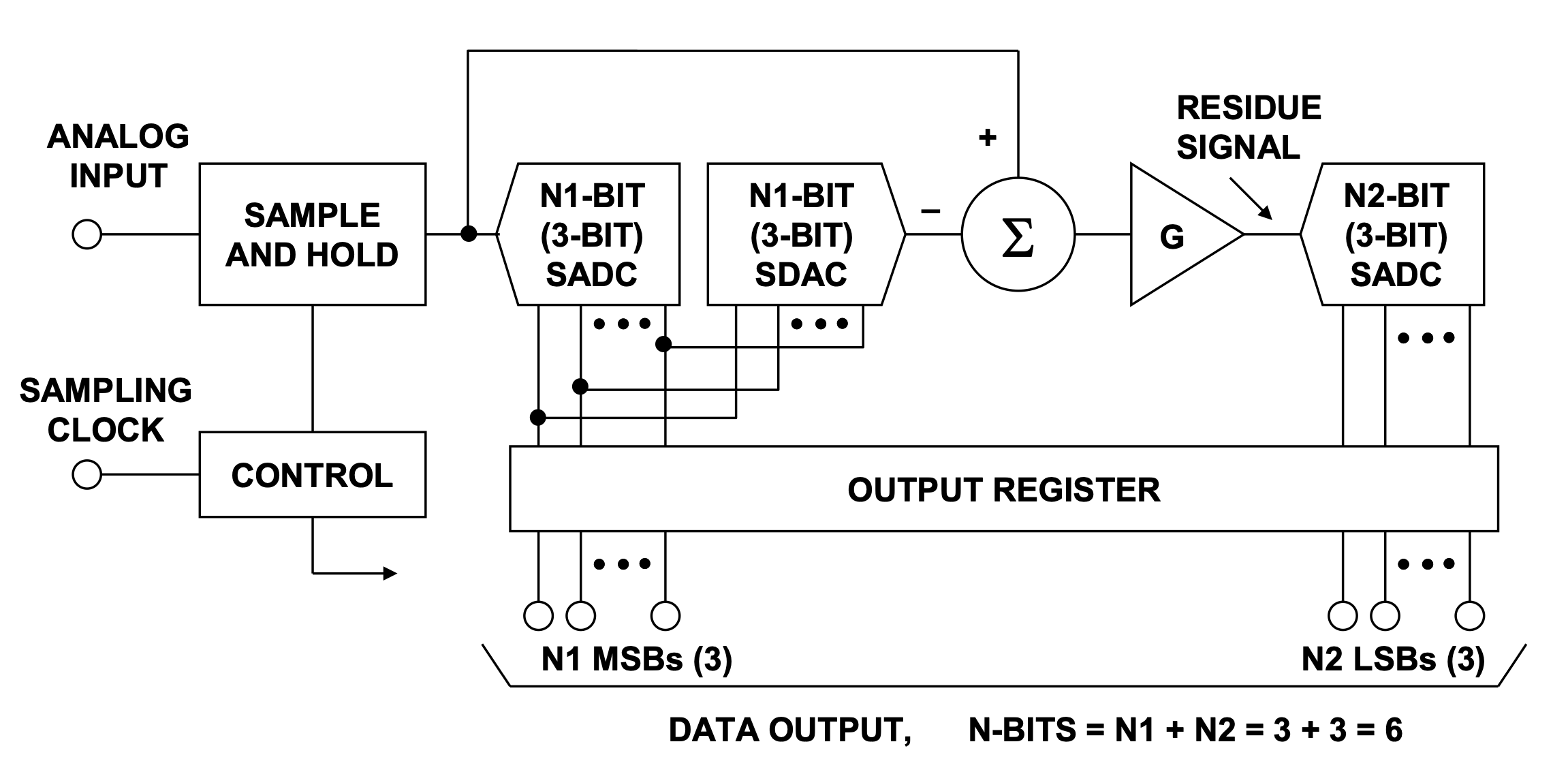
流水线 ADC 通常由 N 个位数相同或不相同的 低分辨率子级组成 ,除最后一级外 ,每个子级都包括 子 ADC 、子 DAC 、减法电路和余量放大器 ,其中子 DAC 、减法电路和余量放大器组合在一起称为 MDAC .
|
||||
|
||||
- 逐次逼近型ADC(SAR)
|
||||
|
||||
多年来,SAR ADC一直是数据采集系统的主流。最近的设计改进将这些ADC的采样频率扩展到兆赫范围,分辨率为18位。模拟设备PulSAR®系列SAR ADC使用内部开关电容技术和自动校准,并在CMOS工艺上以2 MSPS(AD7641)提供18位,无需昂贵的薄膜激光微调。在16位级别,AD7625(6 MSPS)和AD7626(10 MSPS)也代表了突破性的技术。
|
||||
|
||||

|
||||
|
||||
SAR ADC 分多步执行转换, 转换步骤数等 于ADC转换器中的位数。每个步骤均由ADC时钟驱动。每个ADC时钟从结果到输出产生一 位。ADC的内部设计基于切换电容技术。
|
||||
|
||||
以10bit ADC为例
|
||||
|
||||

|
||||
|
||||
1. 采样状态:电容充电至电压VIN。Sa切换至VIN,采样期间Sb开关闭合
|
||||
2. 保持状态:输入断开,电容保持输入电压。Sb开关打开,然后S1-S11切换至接地且Sa切换至VREF。
|
||||
3. 逐次逼近:第一个逼近步骤。S1切换至VREF。VIN与VREF/2比较。如果MSB = 0,则与¼VREF进行比较,S1切换回接地。S2切换至VREF。如果MSB = 1,则与¾VREF进行比较,S1保持接地。S2切换至VREF。重复如上步骤,直到LSB为止。可以简单理解为二分法逐次进行输入电压与参考电压的比较。首次于VREF/2比较,下次比较根据上次比较结果决定,如果MSB=1则与¾VREF比较。如果MSB=0则与¼VREF比较。后面决定与1/8VREF 3/8VREF、 5/8VREF、 7/8VREF之一做比较。循环直到输出LSB为止。
|
||||
|
||||
- ∑–△ ADC
|
||||
|
||||
sigma-delta ADC是现代声带、音频和高分辨率精密工业测量应用的首选转换器。高度数字化的体系结构非常适合现代fine-line CMOS工艺,因此可以在不显著增加成本的情况下轻松添加数字功能。由于它的广泛使用,了解这种转换器架构背后的基本原理非常重要。
|
||||
|
||||

|
||||
|
||||
|
||||
|
||||
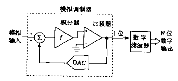
这种ADC又称为过采样转换器,其结构较简单。它由∑–△调制器及连接于其后的数字滤故器构成。调制器的结构近似于双斜率ADC,包括一个积分器和一个比较器,以及含有一个1位DAC的反馈环。这个内置的DAC仅仅是一个开关。它将积分器输入切换到一个正或负的参考电压。∑–△ADC还包括一个时钟单元.为调制器和数字滤波器提供适当的定时。窄带信号送人∑–△ADC后以非常低的分辨率(1位)进行量化,但采样频率却非常高.如2MHz或更高。经过数字滤波处理后 .这种过采样速率被降低到8kHz左右,同时ADC的分辨率(即动态范围 ) 被提高到16位或更高。尽管比流水线ADC慢且输入带宽较窄,∑–△ADC仍具有以下三种优势:
|
||||
|
||||
- 低价格、高性能
|
||||
- 集成化的数字滤波
|
||||
- 与DSP技术兼容,便于实现系统集成
|
||||
|
||||
- 积分型ADC
|
||||
|
||||
|
||||
|
||||
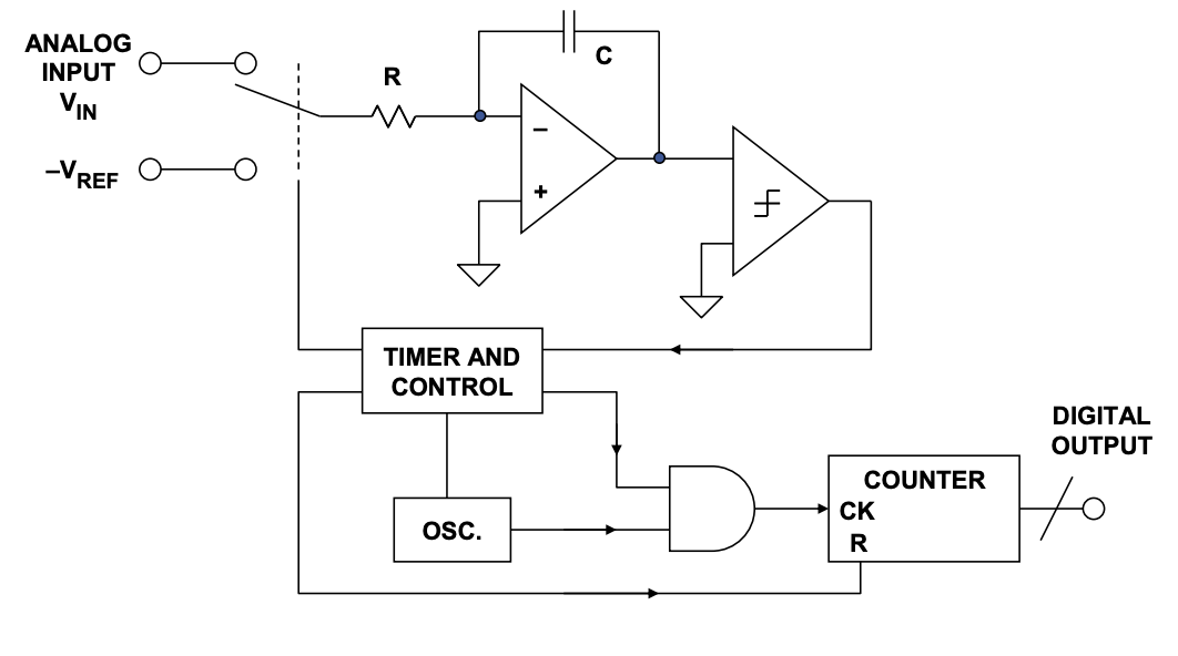
积分型ADC又称双斜率或多斜率数据转换器,是应用最为广泛的转换器类型。经典的双斜率转换器包括两个主要部分:一部分电路采样并量化输入电压.产生一个时域间隔或脉冲序列;再由一个计数器将其转换为数字量输出。双斜率转换器采用一个带有输入切换开头关的模拟积分器,一个比较器和一个计数单元。积分器对输入电压积分固定的时间间隔Tm幢,诙时间间隔通常对应于内部计数单元的最大计数(如图4所示)时间到达后将计数器复位井将积分器输入连接到反极性(负)参考电压。在这个反扳性信号作用下积分器被“反向积分直到括出回到零,井使计数器终止 ,积分器复位。
|
||||
|
||||
- 折叠型ADC (Folding ADC)
|
||||
|
||||
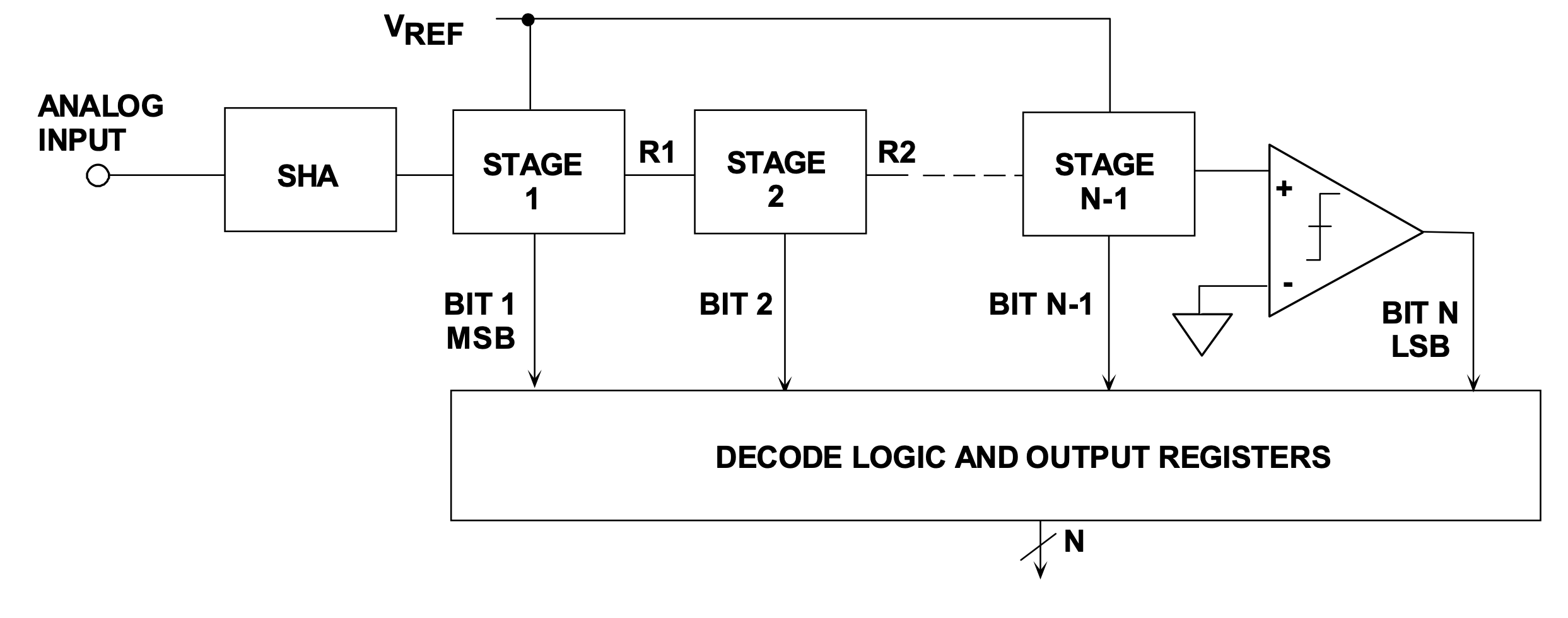
“折叠”架构使用每比特一级执行A/D转换,总体概念如图1所示。每级一位且无纠错的多级流水线ADC基本上是bit-per-stage转换器。实际上,这种类型的流水线转换器通常使用每级1.5bit的方法来提供错误校正。
|
||||
|
||||
|
||||
|
||||
|
||||
|
||||
#### ADC性能指标
|
||||
|
||||
- 面积
|
||||
|
||||
- 功耗
|
||||
|
||||
- 动态范围
|
||||
|
||||
- dBFS
|
||||
|
||||
- THD
|
||||
|
||||
- THD/N
|
||||
|
||||
- SNR
|
||||
|
||||
- DAC SETTLING TIME
|
||||
|
||||
- Glitch impulse area
|
||||
|
||||
|
||||
|
||||
#### ADC误差分析
|
||||
|
||||
要研究ADC数字校准系统,就先要对校准目标有个清晰的认识,明白其误差产生原理,才能针对性去校准误差。 ADC误差主要来源于内部自身转换产生的误差和外部环境造成的误差。
|
||||
|
||||
先简单分析下外部环境误差,外部环境并非在生产和研发阶段可以控制的因素,因此也不在片上校准系统校准范围内, 如参考电压噪声、模拟输入信号噪声、ADC动态范围匹配不佳、模拟信号源电阻、注入电流、温度等影响都会对最后转换精度造成影响。
|
||||
|
||||
- 量化误差
|
||||
|
||||
量化误差是基本误差,用简单3bit ADC来说明。输入电压被数字化,以8个离散电平来划分,分别由代码000b到111b去代表它们,每一代码跨越Vref/8的电压范围。代码大小一般被定义为一个最低有效位(Least Significant Bit,LSB)。若假定Vref=8V时,每个代码之间的电压变换就代表1V。换言之,产生指定代码的实际电压与代表该码的电压两者之间存在误差。一般来说,0.5LSB偏移加入到输入端便导致在理想过渡点上有正负0.5LSB的量化误差。
|
||||
|
||||
- 微分非线性误差
|
||||
|
||||
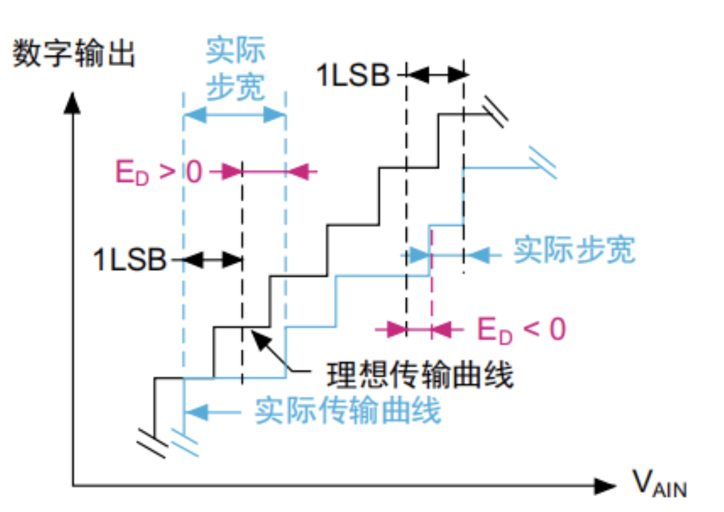
微分线性误差(DLE)为实际步进和理想步进之间的最大偏离。这里的“理想情况”不是指理想传输曲线,而是指ADC分辨率。在下图中,用ED表示DLE。
|
||||
|
||||
ED = 实际步宽 – 1 LSB
|
||||
|
||||
理想情况下,1 LSB的模拟输入电压变化量应导致数字代码变化。如果需要大于1 LSB的模拟输入电压才能导致数字代码变化,将观察到微分线性误差。因此,DLE对应于从一个数字代 码变为下一个数字代码所需的最大额外电压。DLE也称为微分非线性(DLE)误差。
|
||||
|
||||
|
||||
|
||||
- 积分非线性误差
|
||||
|
||||
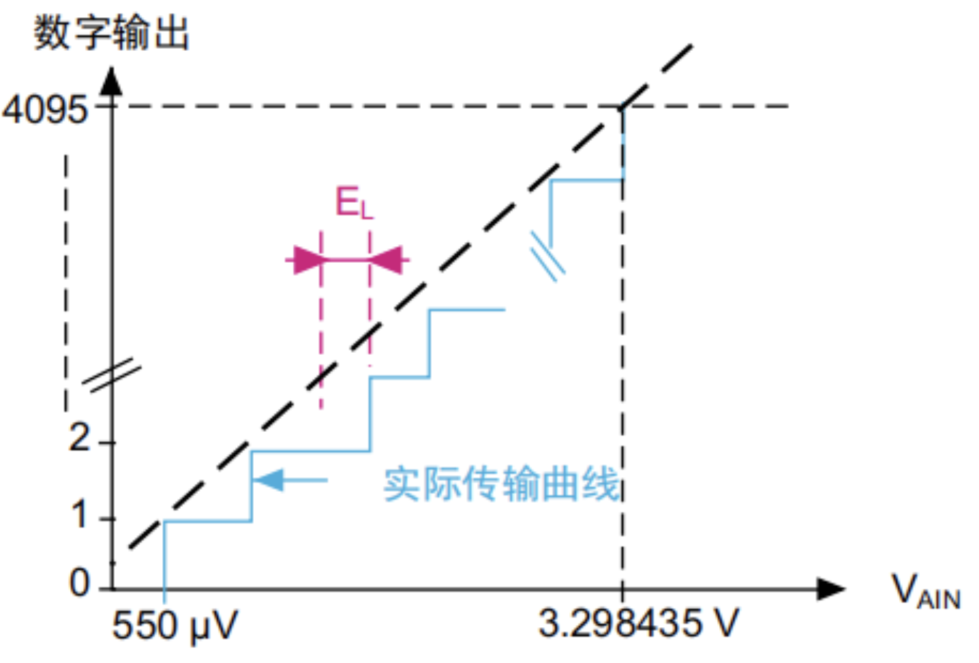
积分线性误差为任何实际转换和端点相关线间的最大偏离。在下图中,用*EL*表示ILE。端点相关线可以定义为A/D传输曲线上连接第一次实际转换与最后一次实际转换的线。*EL*是指与每一次转换的这条线的偏离。因此,端点相关线对应于实际传输曲线并且与理想传输曲线不相关。ILE也称为积分非线性(INL)误差。ILE是整个范围内DLE的积分。
|
||||
|
||||
|
||||
|
||||
- 增益与偏移误差
|
||||
|
||||
偏移误差是第一次实际转换和第一次理想转换之间的偏离。第一次转换发生在数字ADC输出 从0变为1时。理想情况下,当模拟输入介于0.5 LSB和1.5 LSB之间时,数字输出应为1。仍然是理想情况下,第一次转换发生在0.5 LSB处。用EO表示偏移误差。
|
||||
|
||||

|
||||
|
||||
增益误差是最后一次实际转换和最后一次理想转换之间的偏离。增益误差用EG表示。最后一次实际转换是从0xFFE到0xFFF的转换。理想情况下,当模拟输入等于VREF+ – 0.5 LSB时,应存在从0xFFE到0xFFF的转换。因此对于VREF+= 3.3 V,最后一次理想转换应发生 在3.299597 V处。如果ADC提供VAIN < VREF+ – 0.5 LSB的0xFFF读数,将获得负增益误差。
|
||||
|
||||

|
||||
|
||||
|
||||
|
||||
#### ADC 校准方案
|
||||
|
||||
##### 校准系统分类
|
||||
|
||||
- 模拟校准
|
||||
|
||||
使用电路补偿器件误差
|
||||
|
||||
- 数字校准
|
||||
|
||||
- 前台校准
|
||||
|
||||
校准时ADC不工作, 结束后切换
|
||||
|
||||
- 后台校准
|
||||
|
||||
ADC工作同时进行误差校准
|
||||
|
||||
##### 现有校准方法
|
||||
|
||||
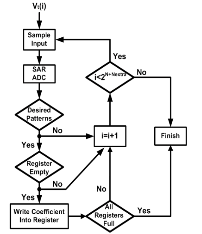
- 基于统计的数字校准
|
||||
|
||||
|
||||
|
||||
- 自适应滤波
|
||||
|
||||
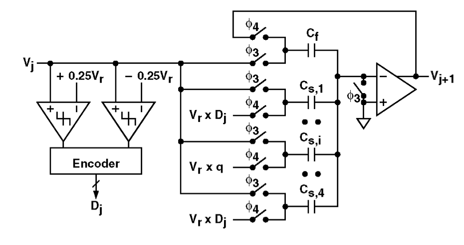
- 多项式插值法
|
||||
|
||||
|
||||
|
||||

|
||||
|
||||
- 有限状态机
|
||||
|
||||
|
||||
|
||||
|
||||
|
||||
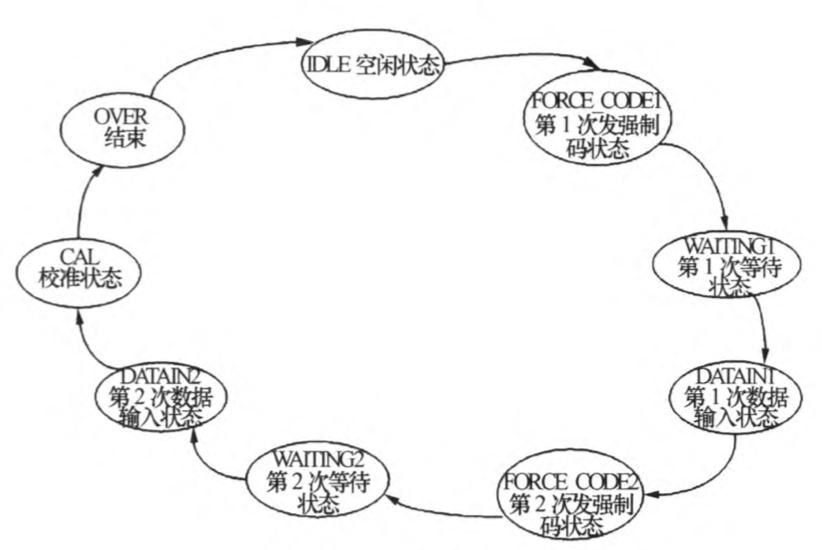
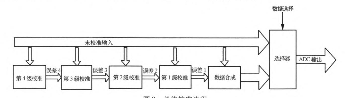
采用有 限状态机的方法一。1刨计算每级校准误差,将每级的校 准信息存入寄存器中。误差运算结束后,将校准参数 对输出码进行校准运算,得到校准后的数字码输出。此数字校准算法可校准对ADC线性影响最大的电容失配误差,适合于1.5 bit级电路和多bit级电 路。明显提高了流水线ADC的无杂散动态范围和有效精度,对模拟电路的改动较小。
|
||||
|
||||
- LMS
|
||||
|
||||
|
||||
|
||||
- 迭代法
|
||||
|
||||
|
||||
|
||||
### 开题 答辩稿
|
||||
|
||||
|
||||
|
||||
1. 各位老师好,我是jll,今天我研究的方向是针对ADC的片上数字校准系统。
|
||||
|
||||
|
||||
|
||||
```
|
||||
Σ-Δ ADC 也可以看作是一个同步电压-频率转换器,后跟一个计数器。如果在足够数量的样本中对输出数据流中“1”的数量进行计数,则计数器输出将表示输入的数字值。
|
||||
```
|
||||
|
||||
```
|
||||
调制器中的积分器表示为模拟低通滤波器,其传递函数等于 H(f) = 1/f。该传递函数具有与输入频率成反比的幅度响应。 1 位量化器生成量化噪声 Q,将其注入输出求和块。如果我们让输入信号为 X,输出 Y,那么从输入加法器出来的信号必须是 X – Y。这乘以滤波器传递函数 1/f,结果进入输出夏天。通过检查,我们可以将输出电压 Y 的表达式写为:
|
||||
请注意,随着频率 f 接近零,输出电压 Y 接近 X 时没有噪声成分。在较高频率下,信号分量的幅度接近零,噪声分量接近 Q。在高频下,输出主要由量化噪声组成。本质上,模拟滤波器对信号有低通作用,对量化噪声有高通作用。因此,模拟滤波器在 Σ-Δ 调制器模型中执行噪声整形功能。
|
||||
```
|
||||
|
||||
|
||||
|
||||
```
|
||||
多级噪声整形 (MASH)
|
||||
```
|
||||
|
||||
|
||||
|
||||
|
||||
|
||||
### 研究方案
|
||||
|
||||
1. 研究目标
|
||||
|
||||
比较现有不同校准算法性能及功耗,针对adc片上校准系统做校准精度、面积、功耗优化
|
||||
|
||||
2. 研究内容
|
||||
|
||||
在20世纪50年代和60年代,直流性能指标(如积分非线性、微分非线性、单调性、无缺失码、增益误差、偏移误差和漂移等)主要用于表征数据转换器。在这个时代,这些规范是足够的,因为大多数早期应用(例如,PCM和雷达除外)处理直流或低频信号,如工业测量和过程控制中遇到的信号。随着20世纪70年代和80年代微处理器和数字信号处理(DSP)的出现,需要动态性能规范,如信噪比(SNR)、无杂散动态范围(SFDR)等,以便充分描述转换器的特性,以用于更复杂的信号处理应用。
|
||||
|
||||
现代数据转换器的应用范围包括从低频工业测量到宽带无线电接收机的频谱。尽管直流规范的重要性通常随着信号频率的增加而降低,但在许多应用中它们仍然很重要。例如,中频采样应用中的显著增益和/或偏移误差可导致信号削波,从而降低SNR和SFDR。在需要匹配转换器的应用中,如交织、同步采样和I/Q信号处理,各个转换器之间的相对增益和偏移匹配至关重要。
|
||||
|
||||
流水线型ADC、逐次逼近型ADC、 ∑–△ ADC是现在比较常用和符合未来发展需要的ADC类型, 各有其优势和特点,研究其校准系统是保证其基本性能和精度的必然要求。为此,深入去研究对比现有方案,探索更多基准性能的校准系统是研究ADC设备的必然一步。
|
||||
|
||||
研究实现现有ADC校准方案,建立统一分析模型,分析其各项性能指标,先做出评测系统,然后针对性的对面积和功耗进行优化,优化现有方案或研究新的方案,争取实现指标突破。
|
||||
|
||||
4. 拟采取的研究方法及可行性分析
|
||||
|
||||
- 阅读相关文献,理解现有校准方案
|
||||
- 根据调研至少确定五种以上校准方案,在fpga上进行硬件实现
|
||||
- 比较每种方案优劣,分析其性能功耗面积
|
||||
- 优化和探索新的实现思路,实现adc校准系统各项指标优化
|
||||
|
||||
|
||||
|
||||
### references
|
||||
|
||||
[1]丁洋, 王宗民. 一种基于统计的流水线ADC数字后台校准方法[J]. 微电子学与计算机, 2011, 28(2):5. [>>>](https://public.veypi.com/research/digitalcalibration/citations/%E4%B8%80%E7%A7%8D%E5%9F%BA%E4%BA%8E%E7%BB%9F%E8%AE%A1%E7%9A%84%E6%B5%81%E6%B0%B4%E7%BA%BFADC%E6%95%B0%E5%AD%97%E5%90%8E%E5%8F%B0%E6%A0%A1%E5%87%86%E6%96%B9%E6%B3%95.pdf)
|
||||
|
||||
[1]郭静宜, 李冬梅, 刘力源,等. 一种适用于流水线ADC的数字校准算法的硬件实现[J]. 高技术通讯, 2009(03):290-294. [>>>](https://public.veypi.com/research/digitalcalibration/citations/%E4%B8%80%E7%A7%8D%E9%80%82%E7%94%A8%E4%BA%8E%E6%B5%81%E6%B0%B4%E7%BA%BFADC%E7%9A%84%E6%95%B0%E5%AD%97%E6%A0%A1%E5%87%86%E7%AE%97%E6%B3%95%E7%9A%84%E7%A1%AC%E4%BB%B6%E5%AE%9E%E7%8E%B0.pdf)
|
||||
|
||||
[1]吴俊杰, 朱从益, 刘海涛. 一种应用于流水线ADC数字校准算法及实现[J]. 现代雷达, 2014, 36(9):44-48. [>>>](https://public.veypi.com/research/digitalcalibration/citations/%E4%B8%80%E7%A7%8D%E5%BA%94%E7%94%A8%E4%BA%8E%E6%B5%81%E6%B0%B4%E7%BA%BFADC%E6%95%B0%E5%AD%97%E6%A0%A1%E5%87%86%E7%AE%97%E6%B3%95%E5%8F%8A%E5%AE%9E%E7%8E%B0.pdf)
|
||||
|
||||
[1]戴澜, 周玉梅, 胡晓宇,等. 一种流水线ADC数字校准算法实现[J]. 半导体学报:英文版, 2008, 29(5):5. [>>>](https://public.veypi.com/research/digitalcalibration/citations/%E4%B8%80%E7%A7%8D%E9%80%82%E7%94%A8%E4%BA%8E%E6%B5%81%E6%B0%B4%E7%BA%BFADC%E7%9A%84%E6%95%B0%E5%AD%97%E6%A0%A1%E5%87%86%E7%AE%97%E6%B3%95%E7%9A%84%E7%A1%AC%E4%BB%B6%E5%AE%9E%E7%8E%B0.pdf)
|
||||
|
||||
[1]张文莲. 折叠内插ADC中数字校准电路设计[J]. 电子制作, 2020(13):4. [>>>](https://public.veypi.com/research/digitalcalibration/citations/%E6%8A%98%E5%8F%A0%E5%86%85%E6%8F%92ADC%E4%B8%AD%E6%95%B0%E5%AD%97%E6%A0%A1%E5%87%86%E7%94%B5%E8%B7%AF%E8%AE%BE%E8%AE%A1_%E5%BC%A0%E6%96%87%E8%8E%B2.pdf)
|
||||
|
||||
[1]杨一波. 时分交替ADC系统数字校准算法与FPGA实现[D]. 电子科技大学. [>>>](https://public.veypi.com/research/digitalcalibration/citations/%E6%97%B6%E5%88%86%E4%BA%A4%E6%9B%BFADC%E7%B3%BB%E7%BB%9F%E6%95%B0%E5%AD%97%E6%A0%A1%E5%87%86%E7%AE%97%E6%B3%95%E4%B8%8EFPGA%E5%AE%9E%E7%8E%B0.pdf)
|
||||
|
||||
[1]宫月红, 罗敏, 金杰. 流水线型ADC误差及相应校正策略研究[J]. 微电子学与计算机, 2014(5).
|
||||
|
||||
[1]贾英江, 王维斌. ADC综述[J]. 电子测量技术, 1999, 000(004):10-13.
|
||||
|
||||
[1] Fukazawa M , Oshima T , Fujiwara M , et al. A CT 2-2 MASH Δ Σ ADC With Multi-Rate LMS-Based Background Calibration and Input-Insensitive Quantization-Error Extraction[J]. IEEE Journal of Solid-State Circuits, 2021, PP(99):1-1. [>>>](https://public.veypi.com/research/digitalcalibration/citations/A%20CT%202-2%20MASH%20--%20ADC%20With%20Multi-Rate%20LMS-Based%20Background%20Calibration%20and%20Input-Insensitive%20Quantization-Error%20Extraction.pdf)
|
||||
|
||||
[1]Moon, Un-Ko, Bang-Sup, et al. Background digital calibration techniques for pipelined ADC's.[J]. IEEE Transactions on Circuits & Systems Part II: Analog & Digital Signal Processing, 1997, 44(2):102-102. [>>>](https://public.veypi.com/research/digitalcalibration/citations/Background%20Digital%20Calibration%20Techniques%20for%20Pipelined%20ADC%E2%80%99s.pdf)
|
||||
|
||||
[1] Wei L , Tao W , Temes G C . Digital foreground calibration methods for SAR ADCs[C]// IEEE. IEEE, 2012. [>>>](https://public.veypi.com/research/digitalcalibration/citations/Digital%20Foreground%20Calibration%20Methods%20for%20SAR%20ADCs%20.pdf)
|
||||
|
||||
[1]Grace, C. R , Hurst, et al. A 12-bit 80-MSample/s pipelined ADC with bootstrapped digital calibration[J]. Solid-State Circuits, IEEE Journal of, 2005, 40(5):1038-1046. [>>>](https://public.veypi.com/research/digitalcalibration/citations/A%2012-bit%2080-Msample%3As%20Pipelined%20ADC%20with%20Bootstrapped%20Digital%20Calibration.pdf)
|
||||
|
||||
[1] Lee Z M , Wang C Y , Wu J T . A CMOS 15-bit 125-MS/s Time-Interleaved ADC With Digital Background Calibration[J]. IEEE Journal of Solid-State Circuits, 2007, 42(10):2149-2160. [>>>](https://public.veypi.com/research/digitalcalibration/citations/a%20cmos%2015-bit%20125-ms%3As%20Time-Interleaved%20ADC%20with%20Digital%20Background%20Calibration.pdf)
|
||||
|
||||
[1] Shu Y S . Background digital calibration techniques for high-speed, high resolution analog-to-digital data converters[J]. Dissertations & Theses, 2008. [>>>](https://public.veypi.com/research/digitalcalibration/citations/Background%20digital%20calibration%20techniques%20for%20high-speed%2C%20high%20resolution%20analog-to-digital%20data%20converters.pdf)
|
||||
|
||||
[1] B lecker, E. B , Mcdonald T M , Erdogan O E , et al. Digital Background Calibration of an Algorithmic Analog-to-Digital Converter Using a Simplified Queue[J]. IEEE Journal of Solid-State Circuits, 2003, 38(6):p.1059-1062.
|
||||
|
||||
[1] [数据转换器学习与设计](https://www.zhihu.com/column/c_1308071540374753280)
|
||||
|
||||
[1] [Time-Interleaved Analog-to-Digital Converters](Time-Interleaved Analog-to-Digital Converters)
|
||||
|
||||
- [sar adc](https://www.cnblogs.com/nevel/p/6151671.html)
|
||||
- [adc category](https://blog.csdn.net/ZQ07506149/article/details/82557492)
|
||||
- [adc error](https://www.21ic.com/article/849518.html)
|
||||
- [∑–△](https://www.cnblogs.com/nevel/p/6152340.html)
|
||||
- [Taking the Mystery out of the Infamous Formula, "SNR = 6.02N + 1.76dB," and Why You Should Care](https://www.analog.com/media/en/training-seminars/tutorials/MT-001.pdf)
|
||||
- [What the Nyquist Criterion Means to Your Sampled Data System Design ](https://www.analog.com/media/en/training-seminars/tutorials/MT-002.pdf)
|
||||
- [Understand SINAD, ENOB, SNR, THD, THD + N, and SFDR so You Don't Get Lost in the Noise Floor ](https://www.analog.com/media/en/training-seminars/tutorials/MT-003.pdf)
|
||||
- [The Good, the Bad, and the Ugly Aspects of ADC Input Noise—Is No Noise Good Noise? ](https://www.analog.com/media/en/training-seminars/tutorials/MT-004.pdf)
|
||||
- [Noise Power Ratio (NPR)—A 65-Year Old Telephone System Specification Finds New Life in Modern Wireless Applications](https://www.analog.com/media/en/training-seminars/tutorials/MT-005.pdf)
|
||||
- [ADC Noise Figure—An Often Misunderstood and Misinterpreted Specification](https://www.analog.com/media/en/training-seminars/tutorials/MT-006.pdf)
|
||||
- [Aperture Time, Aperture Jitter, Aperture Delay Time— Removing the Confusion](https://www.analog.com/media/en/training-seminars/tutorials/MT-007.pdf)
|
||||
- [Converting Oscillator Phase Noise to Time Jitter](https://www.analog.com/media/en/training-seminars/tutorials/MT-008.pdf)
|
||||
- [Data Converter Codes—Can You Decode Them?](https://www.analog.com/media/en/training-seminars/tutorials/MT-009.pdf)
|
||||
- [The Importance of Data Converter Static Specifications— Don't Lose Sight of the Basics!](https://www.analog.com/media/en/training-seminars/tutorials/MT-010.pdf)
|
||||
- [Find Those Elusive ADC Sparkle Codes and Metastable States ](https://www.analog.com/media/en/training-seminars/tutorials/MT-011.pdf)
|
||||
- [隔离](https://www.analog.com/en/analog-dialogue/raqs/raq-issue-189.html)
|
||||
|
||||
- [行业分析](https://finance.sina.com.cn/stock/stockzmt/2021-08-07/doc-ikqciyzm0070703.shtml)
|
||||
- [An Inside Look at High-Speed ADC Accuracy](https://www.electronicdesign.com/technologies/adc/article/21800833/an-inside-look-at-highspeed-adc-accuracy)
|
||||
|
||||
|
||||
+137
@@ -0,0 +1,137 @@
|
||||
@article{丁洋2011一种基于统计的流水线,
|
||||
title={一种基于统计的流水线ADC数字后台校准方法},
|
||||
author={丁洋 and 王宗民},
|
||||
journal={微电子学与计算机},
|
||||
volume={28},
|
||||
number={2},
|
||||
pages={5},
|
||||
year={2011},
|
||||
}
|
||||
|
||||
|
||||
@article{郭静宜2009一种适用于流水线,
|
||||
title={一种适用于流水线ADC的数字校准算法的硬件实现},
|
||||
author={郭静宜 and 李冬梅 and 刘力源 and 李福乐},
|
||||
journal={高技术通讯},
|
||||
number={03},
|
||||
pages={290-294},
|
||||
year={2009},
|
||||
}
|
||||
|
||||
@article{吴俊杰2014一种应用于流水线,
|
||||
title={一种应用于流水线ADC数字校准算法及实现},
|
||||
author={吴俊杰 and 朱从益 and 刘海涛},
|
||||
journal={现代雷达},
|
||||
volume={36},
|
||||
number={9},
|
||||
pages={44-48},
|
||||
year={2014},
|
||||
}
|
||||
|
||||
@article{戴澜2008一种流水线,
|
||||
title={一种流水线ADC数字校准算法实现},
|
||||
author={戴澜 and 周玉梅 and 胡晓宇 and 蒋见花},
|
||||
journal={半导体学报:英文版},
|
||||
volume={29},
|
||||
number={5},
|
||||
pages={5},
|
||||
year={2008},
|
||||
}
|
||||
|
||||
@article{张文莲2020折叠内插,
|
||||
title={折叠内插ADC中数字校准电路设计},
|
||||
author={张文莲},
|
||||
journal={电子制作},
|
||||
number={13},
|
||||
pages={4},
|
||||
year={2020},
|
||||
}
|
||||
|
||||
@phdthesis{杨一波0时分交替,
|
||||
title={时分交替ADC系统数字校准算法与FPGA实现},
|
||||
author={杨一波},
|
||||
school={电子科技大学},
|
||||
}
|
||||
|
||||
@article{2021A,
|
||||
title={A CT 2-2 MASH Δ Σ ADC With Multi-Rate LMS-Based Background Calibration and Input-Insensitive Quantization-Error Extraction},
|
||||
author={ Fukazawa, M. and Oshima, T. and Fujiwara, M. and Tateyama, K. and Matsui, T. },
|
||||
journal={IEEE Journal of Solid-State Circuits},
|
||||
volume={PP},
|
||||
number={99},
|
||||
pages={1-1},
|
||||
year={2021},
|
||||
}
|
||||
|
||||
@article{Moon1997Background,
|
||||
title={Background digital calibration techniques for pipelined ADC's.},
|
||||
author={Moon and Un-Ko and Bang-Sup and Song},
|
||||
journal={IEEE Transactions on Circuits & Systems Part II: Analog & Digital Signal Processing},
|
||||
volume={44},
|
||||
number={2},
|
||||
pages={102-102},
|
||||
year={1997},
|
||||
}
|
||||
|
||||
@inproceedings{2012Digital,
|
||||
title={Digital foreground calibration methods for SAR ADCs},
|
||||
author={ Wei, L. and Tao, W. and Temes, G. C. },
|
||||
booktitle={IEEE},
|
||||
year={2012},
|
||||
}
|
||||
|
||||
@article{Grace2005A,
|
||||
title={A 12-bit 80-MSample/s pipelined ADC with bootstrapped digital calibration},
|
||||
author={Grace and C., R. and Hurst and P., J. and Lewis and S., H. },
|
||||
journal={Solid-State Circuits, IEEE Journal of},
|
||||
volume={40},
|
||||
number={5},
|
||||
pages={1038-1046},
|
||||
year={2005},
|
||||
}
|
||||
|
||||
|
||||
|
||||
|
||||
|
||||
|
||||
@MISC{_backgrounddi3gital,
|
||||
author = {},
|
||||
title = {Background Digital Calibration Techniques for Pipelined ADC’s},
|
||||
year = {}
|
||||
}
|
||||
|
||||
@article{2007A,
|
||||
title={A CMOS 15-bit 125-MS/s Time-Interleaved ADC With Digital Background Calibration},
|
||||
author={ Lee, Z. M. and Wang, C. Y. and Wu, J. T. },
|
||||
journal={IEEE Journal of Solid-State Circuits},
|
||||
volume={42},
|
||||
number={10},
|
||||
pages={2149-2160},
|
||||
year={2007},
|
||||
}
|
||||
@article{2008Background,
|
||||
title={Background digital calibration techniques for high-speed, high resolution analog-to-digital data converters},
|
||||
author={ Shu, Yun Shiang },
|
||||
journal={Dissertations & Theses},
|
||||
year={2008},
|
||||
}
|
||||
|
||||
|
||||
@article{宫月红2014流水线型,
|
||||
title={流水线型ADC误差及相应校正策略研究},
|
||||
author={宫月红 and 罗敏 and 金杰},
|
||||
journal={微电子学与计算机},
|
||||
number={5},
|
||||
year={2014},
|
||||
}
|
||||
|
||||
@article{贾英江1999ADC,
|
||||
title={ADC综述},
|
||||
author={贾英江 and 王维斌},
|
||||
journal={电子测量技术},
|
||||
volume={000},
|
||||
number={004},
|
||||
pages={10-13},
|
||||
year={1999},
|
||||
}
|
||||
Binary file not shown.
@@ -0,0 +1,40 @@
|
||||
# references
|
||||
|
||||
|
||||
|
||||
- [Taking the Mystery out of the Infamous Formula, "SNR = 6.02N + 1.76dB," and Why You Should Care](https://www.analog.com/media/en/training-seminars/tutorials/MT-001.pdf)
|
||||
- [What the Nyquist Criterion Means to Your Sampled Data System Design ](https://www.analog.com/media/en/training-seminars/tutorials/MT-002.pdf)
|
||||
- [Understand SINAD, ENOB, SNR, THD, THD + N, and SFDR so You Don't Get Lost in the Noise Floor ](https://www.analog.com/media/en/training-seminars/tutorials/MT-003.pdf)
|
||||
- [The Good, the Bad, and the Ugly Aspects of ADC Input Noise—Is No Noise Good Noise? ](https://www.analog.com/media/en/training-seminars/tutorials/MT-004.pdf)
|
||||
- [Noise Power Ratio (NPR)—A 65-Year Old Telephone System Specification Finds New Life in Modern Wireless Applications](https://www.analog.com/media/en/training-seminars/tutorials/MT-005.pdf)
|
||||
- [ADC Noise Figure—An Often Misunderstood and Misinterpreted Specification](https://www.analog.com/media/en/training-seminars/tutorials/MT-006.pdf)
|
||||
- [Aperture Time, Aperture Jitter, Aperture Delay Time— Removing the Confusion](https://www.analog.com/media/en/training-seminars/tutorials/MT-007.pdf)
|
||||
- [Converting Oscillator Phase Noise to Time Jitter](https://www.analog.com/media/en/training-seminars/tutorials/MT-008.pdf)
|
||||
- [Data Converter Codes—Can You Decode Them?](https://www.analog.com/media/en/training-seminars/tutorials/MT-009.pdf)
|
||||
- [The Importance of Data Converter Static Specifications— Don't Lose Sight of the Basics!](https://www.analog.com/media/en/training-seminars/tutorials/MT-010.pdf)
|
||||
- [Find Those Elusive ADC Sparkle Codes and Metastable States ](https://www.analog.com/media/en/training-seminars/tutorials/MT-011.pdf)
|
||||
- [Intermodulation Distortion Considerations for ADCs ](https://www.analog.com/media/en/training-seminars/tutorials/MT-012.pdf)
|
||||
- [Evaluating High Speed DAC Performance ](https://www.analog.com/media/en/training-seminars/tutorials/MT-013.pdf)
|
||||
- [Basic DAC Architectures I: String DACs and Thermometer (Fully Decoded) DACs ](https://www.analog.com/media/en/training-seminars/tutorials/MT-014.pdf)
|
||||
- [Basic DAC Architectures II: Binary DACs](https://www.analog.com/media/en/training-seminars/tutorials/MT-015.pdf)
|
||||
- [Basic DAC Architectures III: Segmented DACs](https://www.analog.com/media/en/training-seminars/tutorials/MT-016.pdf)
|
||||
- [Oversampling Interpolating](https://www.analog.com/media/en/training-seminars/tutorials/MT-017.pdf)
|
||||
- [Intentionally Nonlinear DACs](https://www.analog.com/media/en/training-seminars/tutorials/MT-018.pdf)
|
||||
- [DAC Interface Fundamentals ](https://www.analog.com/media/en/training-seminars/tutorials/MT-019.pdf)
|
||||
- [ADC Architectures I: The Flash Converter](https://www.analog.com/media/en/training-seminars/tutorials/MT-020.pdf)
|
||||
- [ADC Architectures II: Successive Approximation ADCs ](https://www.analog.com/media/en/training-seminars/tutorials/MT-021.pdf)
|
||||
- [ADC Architectures III: Sigma-Delta ADC Basics ](https://www.analog.com/media/en/training-seminars/tutorials/MT-022.pdf)
|
||||
- [ADC Architectures IV: Sigma-Delta ADC Advanced Concepts and Applications ](https://www.analog.com/media/en/training-seminars/tutorials/MT-023.pdf)
|
||||
- [ADC Architectures V: Pipelined Subranging ADCs](https://www.analog.com/media/en/training-seminars/tutorials/MT-024.pdf)
|
||||
- [ADC Architectures VI: Folding ADCs ](https://www.analog.com/media/en/training-seminars/tutorials/MT-025.pdf)
|
||||
- [ADC Architectures VII: Counting ADCs](https://www.analog.com/media/en/training-seminars/tutorials/MT-026.pdf)
|
||||
- [ADC Architectures VIII: Integrating ADCs ](https://www.analog.com/media/en/training-seminars/tutorials/MT-027.pdf)
|
||||
- [Voltage-to-Frequency Converters](https://www.analog.com/media/en/training-seminars/tutorials/MT-028.pdf)
|
||||
- [Optical Encoders ](https://www.analog.com/media/en/training-seminars/tutorials/MT-029.pdf)
|
||||
- [Resolver-to-Digital Converters](https://www.analog.com/media/en/training-seminars/tutorials/MT-030.pdf)
|
||||
- [Grounding Data Converters and Solving the Mystery of "AGND" and "DGND" ](https://www.analog.com/media/en/training-seminars/tutorials/MT-031.pdf)
|
||||
|
||||
[sigma delta ADC原理分析](https://blog.csdn.net/qq_39815222/article/details/103248394)
|
||||
|
||||
[sigma delta 理解程序](https://www.analog.com/en/design-center/interactive-design-tools/sigma-delta-adc-tutorial.html)
|
||||
|
||||
@@ -0,0 +1,95 @@
|
||||
module div_fsm
|
||||
#(
|
||||
parameter DATAWIDTH=8
|
||||
)
|
||||
(
|
||||
input clk ,
|
||||
input rstn ,
|
||||
input en ,
|
||||
output wire ready ,
|
||||
input [DATAWIDTH-1:0] dividend ,
|
||||
input [DATAWIDTH-1:0] divisor ,
|
||||
output wire [DATAWIDTH-1:0] quotient ,
|
||||
output wire [DATAWIDTH-1:0] remainder,
|
||||
output wire vld_out
|
||||
);
|
||||
|
||||
reg [DATAWIDTH*2-1:0] dividend_e ;
|
||||
reg [DATAWIDTH*2-1:0] divisor_e ;
|
||||
reg [DATAWIDTH-1:0] quotient_e ;
|
||||
reg [DATAWIDTH-1:0] remainder_e;
|
||||
|
||||
|
||||
reg [1:0] current_state,next_state;
|
||||
|
||||
reg [DATAWIDTH-1:0] count;
|
||||
|
||||
parameter IDLE =2'b00 ,
|
||||
SUB =2'b01 ,
|
||||
SHIFT=2'b10 ,
|
||||
DONE =2'b11 ;
|
||||
|
||||
|
||||
|
||||
always@(posedge clk or negedge rstn)
|
||||
if(!rstn) current_state <= IDLE;
|
||||
else current_state <= next_state;
|
||||
|
||||
always @(*) begin
|
||||
next_state <= 2'bx;
|
||||
case(current_state)
|
||||
IDLE: if(en) next_state <= SUB;
|
||||
else next_state <= IDLE;
|
||||
SUB: next_state <= SHIFT;
|
||||
SHIFT:if(count<DATAWIDTH) next_state <= SUB;
|
||||
else next_state <= DONE;
|
||||
DONE: next_state <= IDLE;
|
||||
endcase
|
||||
end
|
||||
|
||||
|
||||
always@(posedge clk or negedge rstn) begin
|
||||
if(!rstn)begin
|
||||
dividend_e <= 0;
|
||||
divisor_e <= 0;
|
||||
quotient_e <= 0;
|
||||
remainder_e <= 0;
|
||||
count <= 0;
|
||||
end
|
||||
else begin
|
||||
case(current_state)
|
||||
IDLE:begin
|
||||
dividend_e <= {{DATAWIDTH{1'b0}},dividend};
|
||||
divisor_e <= {divisor,{DATAWIDTH{1'b0}}};
|
||||
end
|
||||
SUB:begin
|
||||
if(dividend_e>=divisor_e)begin
|
||||
quotient_e <= {quotient_e[DATAWIDTH-2:0],1'b1};
|
||||
dividend_e <= dividend_e-divisor_e;
|
||||
end
|
||||
else begin
|
||||
quotient_e <= {quotient_e[DATAWIDTH-2:0],1'b0};
|
||||
dividend_e <= dividend_e;
|
||||
end
|
||||
end
|
||||
SHIFT:begin
|
||||
if(count<DATAWIDTH)begin
|
||||
dividend_e <= dividend_e<<1;
|
||||
count <= count+1;
|
||||
end
|
||||
else begin
|
||||
remainder_e <= dividend_e[DATAWIDTH*2-1:DATAWIDTH];
|
||||
end
|
||||
end
|
||||
DONE:begin
|
||||
count <= 0;
|
||||
end
|
||||
endcase
|
||||
end
|
||||
end
|
||||
|
||||
assign quotient = quotient_e;
|
||||
assign remainder = remainder_e;
|
||||
assign ready=(current_state==IDLE)? 1'b1:1'b0;
|
||||
assign vld_out=(current_state==DONE)? 1'b1:1'b0;
|
||||
endmodule
|
||||
Executable
+355
@@ -0,0 +1,355 @@
|
||||
#! /usr/local/Cellar/icarus-verilog/11.0/bin/vvp
|
||||
:ivl_version "11.0 (stable)";
|
||||
:ivl_delay_selection "TYPICAL";
|
||||
:vpi_time_precision - 12;
|
||||
:vpi_module "/usr/local/Cellar/icarus-verilog/11.0/lib/ivl/system.vpi";
|
||||
:vpi_module "/usr/local/Cellar/icarus-verilog/11.0/lib/ivl/vhdl_sys.vpi";
|
||||
:vpi_module "/usr/local/Cellar/icarus-verilog/11.0/lib/ivl/vhdl_textio.vpi";
|
||||
:vpi_module "/usr/local/Cellar/icarus-verilog/11.0/lib/ivl/v2005_math.vpi";
|
||||
:vpi_module "/usr/local/Cellar/icarus-verilog/11.0/lib/ivl/va_math.vpi";
|
||||
S_0x7f8221f04500 .scope module, "div_int_tb" "div_int_tb" 2 4;
|
||||
.timescale -9 -12;
|
||||
P_0x600000c48240 .param/l "DATAWIDTH" 0 2 6, +C4<00000000000000000000000000010000>;
|
||||
v0x600002b4cd80_0 .var "clk", 0 0;
|
||||
v0x600002b4ce10_0 .var "dividend", 15 0;
|
||||
v0x600002b4cea0_0 .var "divisor", 15 0;
|
||||
v0x600002b4cf30_0 .var "en", 0 0;
|
||||
v0x600002b4cfc0_0 .var/i "i", 31 0;
|
||||
v0x600002b4d050_0 .net "quotient", 15 0, L_0x600003248230; 1 drivers
|
||||
v0x600002b4d0e0_0 .net "quotient_ref", 15 0, L_0x6000028480a0; 1 drivers
|
||||
v0x600002b4d170_0 .net "ready", 0 0, L_0x600002848280; 1 drivers
|
||||
v0x600002b4d200_0 .net "remainder", 15 0, L_0x6000032482a0; 1 drivers
|
||||
v0x600002b4d290_0 .net "remainder_ref", 15 0, L_0x600002848140; 1 drivers
|
||||
v0x600002b4d320_0 .var "rstn", 0 0;
|
||||
v0x600002b4d3b0_0 .net "vld_out", 0 0, L_0x6000028483c0; 1 drivers
|
||||
E_0x6000017482a0 .event edge, v0x600002b4ccf0_0;
|
||||
E_0x6000017482d0 .event edge, v0x600002b4cab0_0;
|
||||
E_0x600001748300 .event posedge, v0x600002b4c480_0;
|
||||
L_0x6000028480a0 .arith/div 16, v0x600002b4ce10_0, v0x600002b4cea0_0;
|
||||
L_0x600002848140 .arith/mod 16, v0x600002b4ce10_0, v0x600002b4cea0_0;
|
||||
S_0x7f8221f04670 .scope module, "U_DIV_FSM_0" "div_fsm" 2 53, 3 1 0, S_0x7f8221f04500;
|
||||
.timescale -9 -12;
|
||||
.port_info 0 /INPUT 1 "clk";
|
||||
.port_info 1 /INPUT 1 "rstn";
|
||||
.port_info 2 /INPUT 1 "en";
|
||||
.port_info 3 /OUTPUT 1 "ready";
|
||||
.port_info 4 /INPUT 16 "dividend";
|
||||
.port_info 5 /INPUT 16 "divisor";
|
||||
.port_info 6 /OUTPUT 16 "quotient";
|
||||
.port_info 7 /OUTPUT 16 "remainder";
|
||||
.port_info 8 /OUTPUT 1 "vld_out";
|
||||
P_0x7f8221f047e0 .param/l "DATAWIDTH" 0 3 3, +C4<00000000000000000000000000010000>;
|
||||
P_0x7f8221f04820 .param/l "DONE" 0 3 30, C4<11>;
|
||||
P_0x7f8221f04860 .param/l "IDLE" 0 3 27, C4<00>;
|
||||
P_0x7f8221f048a0 .param/l "SHIFT" 0 3 29, C4<10>;
|
||||
P_0x7f8221f048e0 .param/l "SUB" 0 3 28, C4<01>;
|
||||
L_0x600003248230 .functor BUFZ 16, v0x600002b4ca20_0, C4<0000000000000000>, C4<0000000000000000>, C4<0000000000000000>;
|
||||
L_0x6000032482a0 .functor BUFZ 16, v0x600002b4cbd0_0, C4<0000000000000000>, C4<0000000000000000>, C4<0000000000000000>;
|
||||
L_0x7f8228050098 .functor BUFT 1, C4<0>, C4<0>, C4<0>, C4<0>;
|
||||
v0x600002b4c000_0 .net/2u *"_ivl_10", 0 0, L_0x7f8228050098; 1 drivers
|
||||
L_0x7f82280500e0 .functor BUFT 1, C4<11>, C4<0>, C4<0>, C4<0>;
|
||||
v0x600002b4c090_0 .net/2u *"_ivl_14", 1 0, L_0x7f82280500e0; 1 drivers
|
||||
v0x600002b4c120_0 .net *"_ivl_16", 0 0, L_0x600002848320; 1 drivers
|
||||
L_0x7f8228050128 .functor BUFT 1, C4<1>, C4<0>, C4<0>, C4<0>;
|
||||
v0x600002b4c1b0_0 .net/2u *"_ivl_18", 0 0, L_0x7f8228050128; 1 drivers
|
||||
L_0x7f8228050170 .functor BUFT 1, C4<0>, C4<0>, C4<0>, C4<0>;
|
||||
v0x600002b4c240_0 .net/2u *"_ivl_20", 0 0, L_0x7f8228050170; 1 drivers
|
||||
L_0x7f8228050008 .functor BUFT 1, C4<00>, C4<0>, C4<0>, C4<0>;
|
||||
v0x600002b4c2d0_0 .net/2u *"_ivl_4", 1 0, L_0x7f8228050008; 1 drivers
|
||||
v0x600002b4c360_0 .net *"_ivl_6", 0 0, L_0x6000028481e0; 1 drivers
|
||||
L_0x7f8228050050 .functor BUFT 1, C4<1>, C4<0>, C4<0>, C4<0>;
|
||||
v0x600002b4c3f0_0 .net/2u *"_ivl_8", 0 0, L_0x7f8228050050; 1 drivers
|
||||
v0x600002b4c480_0 .net "clk", 0 0, v0x600002b4cd80_0; 1 drivers
|
||||
v0x600002b4c510_0 .var "count", 15 0;
|
||||
v0x600002b4c5a0_0 .var "current_state", 1 0;
|
||||
v0x600002b4c630_0 .net "dividend", 15 0, v0x600002b4ce10_0; 1 drivers
|
||||
v0x600002b4c6c0_0 .var "dividend_e", 31 0;
|
||||
v0x600002b4c750_0 .net "divisor", 15 0, v0x600002b4cea0_0; 1 drivers
|
||||
v0x600002b4c7e0_0 .var "divisor_e", 31 0;
|
||||
v0x600002b4c870_0 .net "en", 0 0, v0x600002b4cf30_0; 1 drivers
|
||||
v0x600002b4c900_0 .var "next_state", 1 0;
|
||||
v0x600002b4c990_0 .net "quotient", 15 0, L_0x600003248230; alias, 1 drivers
|
||||
v0x600002b4ca20_0 .var "quotient_e", 15 0;
|
||||
v0x600002b4cab0_0 .net "ready", 0 0, L_0x600002848280; alias, 1 drivers
|
||||
v0x600002b4cb40_0 .net "remainder", 15 0, L_0x6000032482a0; alias, 1 drivers
|
||||
v0x600002b4cbd0_0 .var "remainder_e", 15 0;
|
||||
v0x600002b4cc60_0 .net "rstn", 0 0, v0x600002b4d320_0; 1 drivers
|
||||
v0x600002b4ccf0_0 .net "vld_out", 0 0, L_0x6000028483c0; alias, 1 drivers
|
||||
E_0x600001748330/0 .event negedge, v0x600002b4cc60_0;
|
||||
E_0x600001748330/1 .event posedge, v0x600002b4c480_0;
|
||||
E_0x600001748330 .event/or E_0x600001748330/0, E_0x600001748330/1;
|
||||
E_0x600001748360 .event edge, v0x600002b4c5a0_0, v0x600002b4c870_0, v0x600002b4c510_0;
|
||||
L_0x6000028481e0 .cmp/eq 2, v0x600002b4c5a0_0, L_0x7f8228050008;
|
||||
L_0x600002848280 .functor MUXZ 1, L_0x7f8228050098, L_0x7f8228050050, L_0x6000028481e0, C4<>;
|
||||
L_0x600002848320 .cmp/eq 2, v0x600002b4c5a0_0, L_0x7f82280500e0;
|
||||
L_0x6000028483c0 .functor MUXZ 1, L_0x7f8228050170, L_0x7f8228050128, L_0x600002848320, C4<>;
|
||||
.scope S_0x7f8221f04670;
|
||||
T_0 ;
|
||||
%wait E_0x600001748330;
|
||||
%load/vec4 v0x600002b4cc60_0;
|
||||
%nor/r;
|
||||
%flag_set/vec4 8;
|
||||
%jmp/0xz T_0.0, 8;
|
||||
%pushi/vec4 0, 0, 2;
|
||||
%assign/vec4 v0x600002b4c5a0_0, 0;
|
||||
%jmp T_0.1;
|
||||
T_0.0 ;
|
||||
%load/vec4 v0x600002b4c900_0;
|
||||
%assign/vec4 v0x600002b4c5a0_0, 0;
|
||||
T_0.1 ;
|
||||
%jmp T_0;
|
||||
.thread T_0;
|
||||
.scope S_0x7f8221f04670;
|
||||
T_1 ;
|
||||
%wait E_0x600001748360;
|
||||
%pushi/vec4 3, 3, 2;
|
||||
%assign/vec4 v0x600002b4c900_0, 0;
|
||||
%load/vec4 v0x600002b4c5a0_0;
|
||||
%dup/vec4;
|
||||
%pushi/vec4 0, 0, 2;
|
||||
%cmp/u;
|
||||
%jmp/1 T_1.0, 6;
|
||||
%dup/vec4;
|
||||
%pushi/vec4 1, 0, 2;
|
||||
%cmp/u;
|
||||
%jmp/1 T_1.1, 6;
|
||||
%dup/vec4;
|
||||
%pushi/vec4 2, 0, 2;
|
||||
%cmp/u;
|
||||
%jmp/1 T_1.2, 6;
|
||||
%dup/vec4;
|
||||
%pushi/vec4 3, 0, 2;
|
||||
%cmp/u;
|
||||
%jmp/1 T_1.3, 6;
|
||||
%jmp T_1.4;
|
||||
T_1.0 ;
|
||||
%load/vec4 v0x600002b4c870_0;
|
||||
%flag_set/vec4 8;
|
||||
%jmp/0xz T_1.5, 8;
|
||||
%pushi/vec4 1, 0, 2;
|
||||
%assign/vec4 v0x600002b4c900_0, 0;
|
||||
%jmp T_1.6;
|
||||
T_1.5 ;
|
||||
%pushi/vec4 0, 0, 2;
|
||||
%assign/vec4 v0x600002b4c900_0, 0;
|
||||
T_1.6 ;
|
||||
%jmp T_1.4;
|
||||
T_1.1 ;
|
||||
%pushi/vec4 2, 0, 2;
|
||||
%assign/vec4 v0x600002b4c900_0, 0;
|
||||
%jmp T_1.4;
|
||||
T_1.2 ;
|
||||
%load/vec4 v0x600002b4c510_0;
|
||||
%pad/u 32;
|
||||
%cmpi/u 16, 0, 32;
|
||||
%jmp/0xz T_1.7, 5;
|
||||
%pushi/vec4 1, 0, 2;
|
||||
%assign/vec4 v0x600002b4c900_0, 0;
|
||||
%jmp T_1.8;
|
||||
T_1.7 ;
|
||||
%pushi/vec4 3, 0, 2;
|
||||
%assign/vec4 v0x600002b4c900_0, 0;
|
||||
T_1.8 ;
|
||||
%jmp T_1.4;
|
||||
T_1.3 ;
|
||||
%pushi/vec4 0, 0, 2;
|
||||
%assign/vec4 v0x600002b4c900_0, 0;
|
||||
%jmp T_1.4;
|
||||
T_1.4 ;
|
||||
%pop/vec4 1;
|
||||
%jmp T_1;
|
||||
.thread T_1, $push;
|
||||
.scope S_0x7f8221f04670;
|
||||
T_2 ;
|
||||
%wait E_0x600001748330;
|
||||
%load/vec4 v0x600002b4cc60_0;
|
||||
%nor/r;
|
||||
%flag_set/vec4 8;
|
||||
%jmp/0xz T_2.0, 8;
|
||||
%pushi/vec4 0, 0, 32;
|
||||
%assign/vec4 v0x600002b4c6c0_0, 0;
|
||||
%pushi/vec4 0, 0, 32;
|
||||
%assign/vec4 v0x600002b4c7e0_0, 0;
|
||||
%pushi/vec4 0, 0, 16;
|
||||
%assign/vec4 v0x600002b4ca20_0, 0;
|
||||
%pushi/vec4 0, 0, 16;
|
||||
%assign/vec4 v0x600002b4cbd0_0, 0;
|
||||
%pushi/vec4 0, 0, 16;
|
||||
%assign/vec4 v0x600002b4c510_0, 0;
|
||||
%jmp T_2.1;
|
||||
T_2.0 ;
|
||||
%load/vec4 v0x600002b4c5a0_0;
|
||||
%dup/vec4;
|
||||
%pushi/vec4 0, 0, 2;
|
||||
%cmp/u;
|
||||
%jmp/1 T_2.2, 6;
|
||||
%dup/vec4;
|
||||
%pushi/vec4 1, 0, 2;
|
||||
%cmp/u;
|
||||
%jmp/1 T_2.3, 6;
|
||||
%dup/vec4;
|
||||
%pushi/vec4 2, 0, 2;
|
||||
%cmp/u;
|
||||
%jmp/1 T_2.4, 6;
|
||||
%dup/vec4;
|
||||
%pushi/vec4 3, 0, 2;
|
||||
%cmp/u;
|
||||
%jmp/1 T_2.5, 6;
|
||||
%jmp T_2.6;
|
||||
T_2.2 ;
|
||||
%pushi/vec4 0, 0, 16;
|
||||
%load/vec4 v0x600002b4c630_0;
|
||||
%concat/vec4; draw_concat_vec4
|
||||
%assign/vec4 v0x600002b4c6c0_0, 0;
|
||||
%load/vec4 v0x600002b4c750_0;
|
||||
%concati/vec4 0, 0, 16;
|
||||
%assign/vec4 v0x600002b4c7e0_0, 0;
|
||||
%jmp T_2.6;
|
||||
T_2.3 ;
|
||||
%load/vec4 v0x600002b4c7e0_0;
|
||||
%load/vec4 v0x600002b4c6c0_0;
|
||||
%cmp/u;
|
||||
%flag_or 5, 4;
|
||||
%jmp/0xz T_2.7, 5;
|
||||
%load/vec4 v0x600002b4ca20_0;
|
||||
%parti/s 15, 0, 2;
|
||||
%concati/vec4 1, 0, 1;
|
||||
%assign/vec4 v0x600002b4ca20_0, 0;
|
||||
%load/vec4 v0x600002b4c6c0_0;
|
||||
%load/vec4 v0x600002b4c7e0_0;
|
||||
%sub;
|
||||
%assign/vec4 v0x600002b4c6c0_0, 0;
|
||||
%jmp T_2.8;
|
||||
T_2.7 ;
|
||||
%load/vec4 v0x600002b4ca20_0;
|
||||
%parti/s 15, 0, 2;
|
||||
%concati/vec4 0, 0, 1;
|
||||
%assign/vec4 v0x600002b4ca20_0, 0;
|
||||
%load/vec4 v0x600002b4c6c0_0;
|
||||
%assign/vec4 v0x600002b4c6c0_0, 0;
|
||||
T_2.8 ;
|
||||
%jmp T_2.6;
|
||||
T_2.4 ;
|
||||
%load/vec4 v0x600002b4c510_0;
|
||||
%pad/u 32;
|
||||
%cmpi/u 16, 0, 32;
|
||||
%jmp/0xz T_2.9, 5;
|
||||
%load/vec4 v0x600002b4c6c0_0;
|
||||
%ix/load 4, 1, 0;
|
||||
%flag_set/imm 4, 0;
|
||||
%shiftl 4;
|
||||
%assign/vec4 v0x600002b4c6c0_0, 0;
|
||||
%load/vec4 v0x600002b4c510_0;
|
||||
%addi 1, 0, 16;
|
||||
%assign/vec4 v0x600002b4c510_0, 0;
|
||||
%jmp T_2.10;
|
||||
T_2.9 ;
|
||||
%load/vec4 v0x600002b4c6c0_0;
|
||||
%parti/s 16, 16, 6;
|
||||
%assign/vec4 v0x600002b4cbd0_0, 0;
|
||||
T_2.10 ;
|
||||
%jmp T_2.6;
|
||||
T_2.5 ;
|
||||
%pushi/vec4 0, 0, 16;
|
||||
%assign/vec4 v0x600002b4c510_0, 0;
|
||||
%jmp T_2.6;
|
||||
T_2.6 ;
|
||||
%pop/vec4 1;
|
||||
T_2.1 ;
|
||||
%jmp T_2;
|
||||
.thread T_2;
|
||||
.scope S_0x7f8221f04500;
|
||||
T_3 ;
|
||||
%delay 1000, 0;
|
||||
%load/vec4 v0x600002b4cd80_0;
|
||||
%inv;
|
||||
%store/vec4 v0x600002b4cd80_0, 0, 1;
|
||||
%jmp T_3;
|
||||
.thread T_3;
|
||||
.scope S_0x7f8221f04500;
|
||||
T_4 ;
|
||||
%pushi/vec4 1, 0, 1;
|
||||
%store/vec4 v0x600002b4cd80_0, 0, 1;
|
||||
%pushi/vec4 1, 0, 1;
|
||||
%store/vec4 v0x600002b4d320_0, 0, 1;
|
||||
%pushi/vec4 0, 0, 1;
|
||||
%store/vec4 v0x600002b4cf30_0, 0, 1;
|
||||
%delay 2000, 0;
|
||||
%pushi/vec4 0, 0, 1;
|
||||
%store/vec4 v0x600002b4d320_0, 0, 1;
|
||||
%delay 2000, 0;
|
||||
%pushi/vec4 1, 0, 1;
|
||||
%store/vec4 v0x600002b4d320_0, 0, 1;
|
||||
%pushi/vec4 2, 0, 32;
|
||||
T_4.0 %dup/vec4;
|
||||
%pushi/vec4 0, 0, 32;
|
||||
%cmp/s;
|
||||
%jmp/1xz T_4.1, 5;
|
||||
%jmp/1 T_4.1, 4;
|
||||
%pushi/vec4 1, 0, 32;
|
||||
%sub;
|
||||
%wait E_0x600001748300;
|
||||
%jmp T_4.0;
|
||||
T_4.1 ;
|
||||
%pop/vec4 1;
|
||||
%pushi/vec4 0, 0, 32;
|
||||
%store/vec4 v0x600002b4cfc0_0, 0, 32;
|
||||
T_4.2 ;
|
||||
%load/vec4 v0x600002b4cfc0_0;
|
||||
%cmpi/s 10, 0, 32;
|
||||
%jmp/0xz T_4.3, 5;
|
||||
%pushi/vec4 1, 0, 1;
|
||||
%assign/vec4 v0x600002b4cf30_0, 0;
|
||||
%vpi_func 2 35 "$random" 32 {0 0 0};
|
||||
%pushi/vec4 1000, 0, 32;
|
||||
%mod/s;
|
||||
%pad/s 16;
|
||||
%assign/vec4 v0x600002b4ce10_0, 0;
|
||||
%vpi_func 2 36 "$random" 32 {0 0 0};
|
||||
%pushi/vec4 100, 0, 32;
|
||||
%mod/s;
|
||||
%pad/s 16;
|
||||
%assign/vec4 v0x600002b4cea0_0, 0;
|
||||
T_4.4 ;
|
||||
%load/vec4 v0x600002b4d170_0;
|
||||
%pad/u 32;
|
||||
%pushi/vec4 1, 0, 32;
|
||||
%cmp/e;
|
||||
%flag_get/vec4 4;
|
||||
%cmpi/ne 1, 0, 1;
|
||||
%jmp/0xz T_4.5, 6;
|
||||
%wait E_0x6000017482d0;
|
||||
%jmp T_4.4;
|
||||
T_4.5 ;
|
||||
T_4.6 ;
|
||||
%load/vec4 v0x600002b4d3b0_0;
|
||||
%pad/u 32;
|
||||
%pushi/vec4 1, 0, 32;
|
||||
%cmp/e;
|
||||
%flag_get/vec4 4;
|
||||
%cmpi/ne 1, 0, 1;
|
||||
%jmp/0xz T_4.7, 6;
|
||||
%wait E_0x6000017482a0;
|
||||
%jmp T_4.6;
|
||||
T_4.7 ;
|
||||
%load/vec4 v0x600002b4cfc0_0;
|
||||
%addi 1, 0, 32;
|
||||
%store/vec4 v0x600002b4cfc0_0, 0, 32;
|
||||
%jmp T_4.2;
|
||||
T_4.3 ;
|
||||
%end;
|
||||
.thread T_4;
|
||||
.scope S_0x7f8221f04500;
|
||||
T_5 ;
|
||||
%vpi_call 2 46 "$dumpfile", "test.vcd" {0 0 0};
|
||||
%vpi_call 2 47 "$dumpvars", 32'sb00000000000000000000000000000000, S_0x7f8221f04500 {0 0 0};
|
||||
%delay 1000000, 0;
|
||||
%vpi_call 2 48 "$finish" {0 0 0};
|
||||
%end;
|
||||
.thread T_5;
|
||||
# The file index is used to find the file name in the following table.
|
||||
:file_names 4;
|
||||
"N/A";
|
||||
"<interactive>";
|
||||
"testIntDivider.v";
|
||||
"./intDivider.v";
|
||||
@@ -0,0 +1,65 @@
|
||||
`timescale 1ns/1ps
|
||||
`include "intDivider.v"
|
||||
|
||||
module div_int_tb();
|
||||
|
||||
parameter DATAWIDTH = 16;
|
||||
|
||||
reg clk;
|
||||
reg rstn;
|
||||
reg en;
|
||||
wire ready;
|
||||
reg [DATAWIDTH-1:0] dividend;
|
||||
reg [DATAWIDTH-1:0] divisor;
|
||||
wire [DATAWIDTH-1:0] quotient;
|
||||
wire [DATAWIDTH-1:0] remainder;
|
||||
wire vld_out;
|
||||
|
||||
wire [DATAWIDTH-1:0] quotient_ref; // true result
|
||||
wire [DATAWIDTH-1:0] remainder_ref;
|
||||
assign quotient_ref = dividend/divisor;
|
||||
assign remainder_ref = dividend%divisor;
|
||||
|
||||
always #1 clk = ~clk;
|
||||
|
||||
integer i;
|
||||
initial begin
|
||||
clk = 1;
|
||||
rstn = 1;
|
||||
en = 0;
|
||||
#2 rstn = 0; #2 rstn = 1;
|
||||
repeat(2) @(posedge clk);
|
||||
|
||||
for(i=0;i<10;i=i+1) begin
|
||||
en <= 1;
|
||||
dividend <= $random%1000;
|
||||
divisor <= $random%100;
|
||||
wait (ready == 1);
|
||||
wait (vld_out == 1);
|
||||
end
|
||||
|
||||
|
||||
end
|
||||
|
||||
|
||||
initial begin
|
||||
$dumpfile("test.vcd");
|
||||
$dumpvars(0, div_int_tb);
|
||||
#1000 $finish;
|
||||
end
|
||||
|
||||
div_fsm #(
|
||||
.DATAWIDTH ( DATAWIDTH ))
|
||||
U_DIV_FSM_0(
|
||||
.clk ( clk ),
|
||||
.rstn ( rstn ),
|
||||
.en ( en ),
|
||||
.ready ( ready ),
|
||||
.dividend ( dividend ),
|
||||
.divisor ( divisor ),
|
||||
.quotient ( quotient ),
|
||||
.remainder ( remainder ),
|
||||
.vld_out ( vld_out )
|
||||
);
|
||||
|
||||
endmodule
|
||||
Reference in New Issue
Block a user